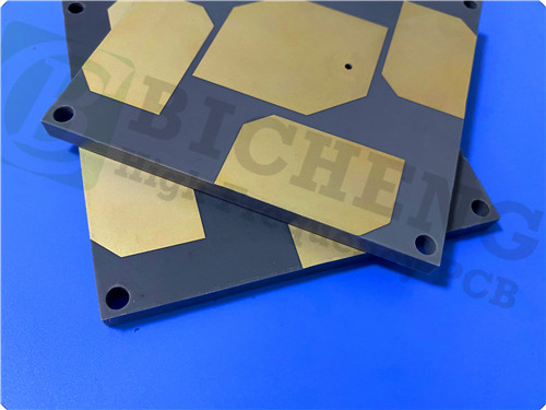
F4BTMS615 High Frequency PCB - 2-Layer Rigid PCB with HASL Finish1.F4BTMS Introduction The F4BTMS series represents an advanced iteration of the F4BTM series, featuring significant innovations in material formulation and manufacturing techniques. This upgraded material incorporates a substantial amount of ceramics and is reinforced with ultra-thin, ultra-fine glass fiber cloth. These enhancements lead to marked improvements in performance and a wider range of dielectric constants, making it a high-reliability option for aerospace applications, capable of replacing similar foreign products. By integrating a small quantity of ultra-thin glass fiber cloth with a large amount of uniformly distributed special nano-ceramics mixed with polytetrafluoroethylene resin, the adverse effects of glass fiber on electromagnetic wave propagation are minimized. This approach reduces dielectric loss, enhances dimensional stability, and decreases the anisotropy in the X/Y/Z directions. It also expands the usable frequency range, improves electrical strength, and boosts thermal conductivity. Furthermore, the material features a low thermal expansion coefficient and stable dielectric temperature characteristics. The F4BTMS series includes RTF low roughness copper foil as a standard feature, which reduces conductor loss and provides excellent peel strength. It is compatible with both copper and aluminum bases.
2. Features of F4BTMS615 Dielectric constant (Dk) of 6.15 at 10 GHz 3. PCB Stackup: 2-layer rigid PCB 4. PCB Construction Details 5. PCB Statistics 6. Type of Artwork Supplied 7. Quality Standard 8. Availability 9. Typical Applications |
Get a Quick Quote
Fill in the form below and our engineers will reply within 24 hours with technical specifications and pricing for F4BTMS615 High Frequency PCB - 2-Layer Rigid PCB with HASL Finish.